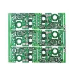
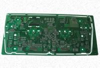
Thickness of 0.8 to 3.2mm (with finished copper of 3 oz for outer layers and 2oz for inner layers), Line width and spacing of 6 6 mils (sample lots 55mils), Minimum finished hole size of 0.3mm, Surface finish of Solder leveling Lead free hot air...
Thickness of 0.8 to 3.2mm (with finished copper of 3 oz for outer layers and 2oz for inner layers), Line width and spacing of 6 6 mils (sample lots 55mils), Minimum finished hole size of 0.3mm, Surface finish of Solder leveling Lead free hot air leveling Chemical Tin ENIG...
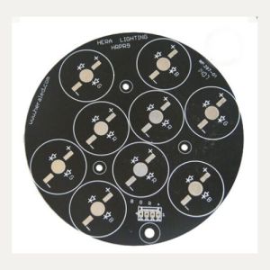
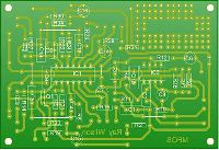
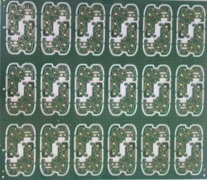
Single sided circuit boards, A printed circuit board with a conductive circuit pattern one side only. Holes in the board are usually not plated through. A printed circuit board, or PCB, is used to mechanically support and electrically connect...
A printed circuit board with a conductive circuit pattern one side only. Holes in the board are usually not plated through. A printed circuit board, or PCB, is used to mechanically support and electrically connect electronic components using conductive pathways, or traces,...
A printed circuit board with a conductive circuit pattern one side only. Holes in the board are usually not plated through. A printed circuit board, or PCB, is used to mechanically support and electrically connect electronic components using...
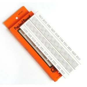
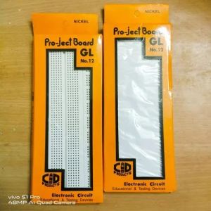
The Best Brand in Protoboard !! Ideal for prototyping and lab work – contact nickel has for durability Ideal for prototyping and electronic laboratory work, it is the most used in digital and microcontrolled analog electronic classes thanks to...


")


