
Company Information
Ask for more detail from the seller
Contact SupplierProduct Name : Single Crystal Silicon Wafer P/N Type 4 inch (Dia)
Pack Size : 5 Pcs, 10 Pcs, 20 Pcs
Silicon Wafer ( P/N-Type )
Boron as a dopant
Type of surface: Single-sided polished
Diameter and thickness: D* = 4 inch and thickness =525±20 μm
Semiconductor properties:
Physical properties: Resistivity: 10 Ω-cm
Product Name : Single Crystal Silicon Wafer P/N Type 3 inch (Dia)
Pack Size : 5 Pcs, 10 Pcs, 20 Pcs
Silicon Wafer ( P/N-Type )
(Orientation):
Type of surface: Single sided polished
Diameter: D* = 3 inch
Thickness = 0.5mm
Semiconductor properties (Orientation):
Resistivity: < 5-10 Ω-cm
Product Name : Single Crystal Silicon Wafer P/N Type 4 inch (Dia)
Silicon Wafer ( N-type/Dopant - Phos. )
Type of surface: Single sided polished
Diameter: D* = 4 inch
Thickness = 525±20 µm
Semiconductor properties (Orientation):
Resistivity: < 10-20 Ω-cm
Product Name : Single Crystal Silicon Wafer P/N Type 2 inch (Dia)
Pack Size : 5 Pcs, 10 Pcs, 20 Pcs
Silicon Wafer ( P/N-Type )
Silicon Wafer
Grade – Prime (Si+Sio2 (wet))
Diameter: D* = 2 inch
Type & Dopant: P Boron
Orientation :
Resistivity: 01-10 Ω-cm
Polished: Single Side polished
Thickness = 380 ± 25 µm
Coating Thickness – 300 nm
Product Name : Single Crystal Silicon Wafer P/N Type 3 inch (Dia)
Pack Size : 5 Pcs, 10 Pcs, 20 Pcs
Silicon Wafer ( P/N-Type )
Grade – Prime (Si+Sio2 (wet))
Diameter: D* = 3 inch
Type & Dopant: N phosphorous/Boron
Orientation:
Resistivity: 01-10 Ω-cm
Polished: Single Side polished
Thickness = 380 ± 25 µm
Coating Thickness – 300 nm
Product Name : Single Crystal Silicon Wafer P/N Type 6 inch (Dia)
Pack Size : 5 Pcs, 10 Pcs, 20 Pcs
Silicon Wafer ( P/N-Type )
Grade – Prime (Si+Sio2 (wet))
Diameter: D* = 6 inch
Type & Dopant: N phosphorous/Boron
Orientation:
Resistivity: 01-10 Ω-cm
Polished: Single Side polished
Thickness = 380 ± 25 µm
Coating Thickness – 300 nm
Description:-
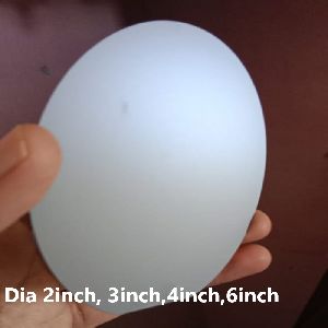
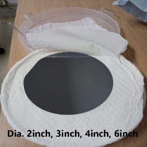
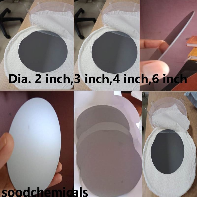
Silicon wafers are available in a variety of sizes ranging from (1 inch) to (6 inches).We want to laser cut the wafer to create a substrate for a microfluidic device and produce thin silicon discs used every month to make products such as integrated circuits and high-performance electronics.This will experience a slight decline due to the fall in silicon prices and the falling demand for the product,Silicon wafer suppliers can be time consuming and difficult to find The best polished Silicon Wafer deals are obtained directly from their suppliers. A wafer is a thin piece of semiconductor material, normally silicon crystal. These wafers are used to fabricate integrated circuits and other micro devices. Silicon wafers are available in a variety of sizes ranging from (1 inch) to (6 inches).
Related Information :-
Storage Conditions:
Airtight Sealed, Avoid light and keep dry at room temperature.


Connect with us