FEATURES
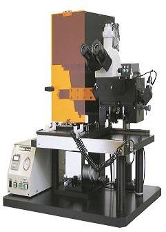
Wafer Size: up to 4” dia Economical, Compact & Hi-Level Performance Viewing fused image of two alignment marks in the field of view. Integrator lens for exposure. LED illuminator
APPLICATIONS
(Micromachine development in R&D center and university) Acuator, Pressure Sensor, Acceleration Sensor, Power Device, etc. Exposure for Flip Chip/BGA/CSP. Exposure for Optical/High Speed Communication Components.
WELCOME TO GLOBAL MARKETING SERVICES, INDIA World has turned flat – thanks to the multifold growth in Satellite communication, internet, desktop computing,and mobile telephony. Innovation in semiconductor technology has been one of the key drivers for this growth. With its rich base of research institutions and various electronics manufacturing companies, India, has emerged to be a hub of innovation in MEMS, Solar and Microelectronics technologies. Sourcing the right semiconductor equipment and manufacturing processes has always been a complex process. Companies find it a challenge to find the right partner who provides technology consulting and efficient product procurement. Global Marketing Services, has been playing a major role in addressing this bottleneck. GMS brings along vast industrial experience and expertise. Over the years GMS, has established successful relationship with some of the leading solution providers and manufacturers of semicon technology in processes and device assembly solutions. GMS adds value to its customers through consultancy, procurement and after sales support.
Nature of Business Manufacturer / Exporter / Supplier / Retailer
Tell us your Buy Requirement to Get Instant Response