Listing ID #3964566
Company Information
Ask for more detail from the seller
Contact SupplierA and B grade solar wafers for cell manufacturing industry can be purchased from SemSil Technologies, Bangalore India.
Our supplies include
- 125 mm mono and multi silicon wafers
- 156 mm pseudo square mono silicon wafers
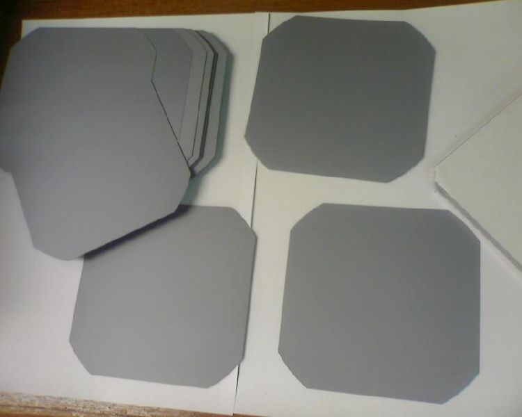
- 156 mm square multi / poly silicon wafers
Semsil Technologies and its group companies are appointed as official distributors for most of the European and Taiwanese wafer producers and 100% quality satisfaction is assured for our clientele.
Our payment terms for Indian cell manufacturers are in Indian Rupee and 100% Letter of Credit terms are accepted. Inco terms are - CIF, any airport in India
156 mm multi silicon wafers
Conductivity Type P-type
Base Area 156 mm X 156 mm
Diagonal 220.0mm±0.5mm;
Thickness 200μm±20μm
TTV(µm) ≤50μm
Resistivity 0.5-3.0Ωcm
Dopant Species Boron
Orientation (100) ±1°
Carbon ≤2.5×10¹⁷ at/cm3
Oxygen ≤1×10¹⁸ at/cm3
Dislocation density ≤3000 / cm2
Life time ≥2μs
Wafer Surface As cut and cleaned. No grease stains and pin holes
Warping ≤50μm
Corner Angle 90±0.5 degree
Edge Chips Length≤1.0mm, Depth<0.5mm
Edge Cracks Not Allowed
Saw marks Depth ≤20μm
Pin Holes No visible pin holes with the naked eye


Connect with us