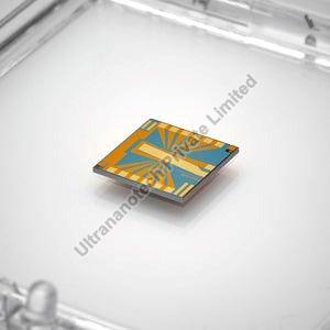
FEATURES Growth method: CVD synthesis Polymer assisted transfer Chip dimensions: 10 mm x 10 mm Chip thickness: 675 μm Number of GFETs per chip: 27 Gate oxide thickness: 90 nm Gate oxide material: SiO2 Dielectric Constant of the SiO2 layer: 3.9 Resistivity of substrate: 1-10 Ω.cm Metallization: Au conmore...
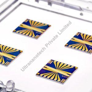
FEATURE GFET-S20 (Die size 10 mm x 10 mm) Processed in Clean Room Class 1000 Growth method: CVD synthesis Polymer assisted transfer Chip dimensions: 10 mm x 10 mm Chip thickness: 675 μm Number of GFETs per chip: 12 Gate oxide thickness: 90 nm Gate oxide material: SiO2 Resistivity of substrate: 1-10 Ωmore...