Business Type


Get Best Sellers for
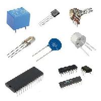
Silicon Wafers
Connect with us