Business Type


Get Best Sellers for
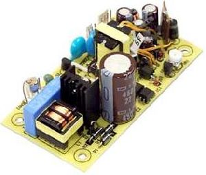
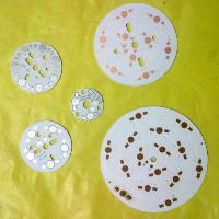
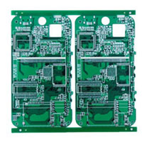
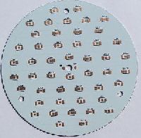
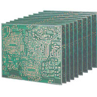
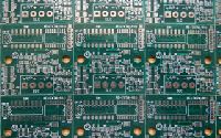
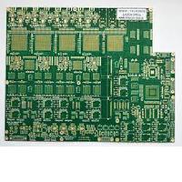
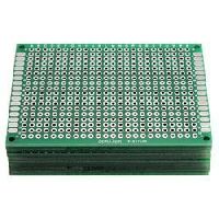
Non PTH PCB
Connect with us